Chipchain Carried Out the Tape-out on 16nm TSMC FinFET Process Technology
Chipchain Carried Out the Tape-out on 16nm TSMC FinFET Process Technology
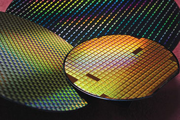
After TSMC’s licensing of 16nm process PDK, Chipchian’s R&D team took about 4 months to quickly complete the design, optimization and verification. The GDS data was submitted to TSMC and Chipchian carried 16nm MPW Shuttle for tape-out on November 6, 2018.
The TSMC CyberShuttle prototyping service is to place multiple integrated circuit designs with the same process technology on the same wafer. Each design can get dozens of chip samples for experiments and verification tests in the product development stage. The tape-out cost is shared by all participating MPW projects according to the area occupied by the chip, which greatly reduces the cost of the integrated circuit development stage. This service has provided a relatively relaxed condition for R&D engineers to conduct deep probe and practice, which effectively promoted the great innovation of R&D design in Chipchain.