
Fabless AI chip company
Full-custom AI chip design at 7 nm and 6 nm.
As a TSMC direct account, Chipchain is authorised for 7 nm FinFET design and has carried out 6 nm AI full-custom chip design for a top AI customer.
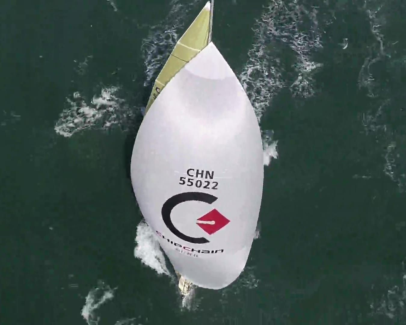
 CHIPCHAIN Team · 13th China Cup International Regatta · Shenzhen, November 2019
- Founded in Shenzhen and Taipei
- 2018
- Our latest process. An MPW tape-out in our founding year and a full-mask tape-out the next year, both on FinFET
- 6 nm
- FinFET process nodes in our design work: 16 nm, 12 nm, 7 nm and 6 nm
- 4
- Direct account
- TSMC
Full-custom and library characterization
Transistor-level design, where it moves the whole chip.
Full-custom applies to the critical datapath blocks; the rest of a chip uses a standard tool flow. From custom cells, library characterization and re-characterization to hand-crafted netlists, custom clock trees and manual place and route, our method has nine stages, and each closes with evidence a customer can read.
7 nm and 6 nm
Authorised for TSMC 7 nm FinFET design; 6 nm AI full-custom chip design carried out for a top AI customer
Library characterization
Standard cell library characterization, including ultra-low-voltage libraries
FinFET tape-outs
The full-custom method on real silicon, from an MPW in our founding year to a full mask set the next year
Nine stages
From fit and partitioning to silicon correlation
What we do
One team for the chip and everything it takes to ship it.
Full-custom and library characterization
Custom cells, library characterization and re-characterization, hand-crafted netlists, custom clock trees and manual place and route, for the blocks that decide a chip's performance.
Custom AI silicon
Accelerators shaped around your models, your power budget and your cost target.
ASIC design services
Architecture, RTL, verification, DFT and physical design, as a full flow or one stage at a time.
Production and supply
Wafers, test, assembly and logistics planned as one schedule.
Engagement models
Hand over as much of the flow as suits your team.
Four starting points. In each, Chipchain owns every stage from the hand-off onward.
| Specification | RTL | Verification | Physical design | Tape-out | Production | |
|---|---|---|---|---|---|---|
| Spec-inYou bring the requirements; we deliver production silicon. | Chipchain | Chipchain | Chipchain | Chipchain | Chipchain | Chipchain |
| Netlist-inYou hand over a verified netlist; we close the design and build it. | Your team | Your team | Chipchain | Chipchain | Chipchain | Chipchain |
| GDS-inYou hand over signed-off layout; we tape it out and run production. | Your team | Your team | Your team | Your team | Chipchain | Chipchain |
| Production transferAn existing chip moves to us for production management. | Your team | Your team | Your team | Your team | Your team | Chipchain |
- Spec-inYou bring the requirements; we deliver production silicon.ChipchainSpecification, RTL, Verification, Physical design, Tape-out, and Production
- Netlist-inYou hand over a verified netlist; we close the design and build it.ChipchainVerification, Physical design, Tape-out, and Production
- GDS-inYou hand over signed-off layout; we tape it out and run production.ChipchainTape-out and Production
- Production transferAn existing chip moves to us for production management.ChipchainProduction
Production and supply
From wafer to shelf, on one plan.
- 01WaferCapacity booked with the foundry.
- 02Wafer probeEvery die tested before it is cut.
- 03AssemblyDies packaged to your footprint.
- 04Final testPackaged parts tested to specification.
- 05QualityLots checked and traceable.
- 06DeliveryStock held and shipped to plan.
Markets
Where custom silicon pays for itself.
Milestones
Built on FinFET since 2018.
Incorporated in Shenzhen and Taipei
Access to a 16 nm FinFET process
12 nm FinFET design kit
First 16 nm tape-out, on a multi-project wafer
16 nm full-mask tape-out
Authorised to use 7 nm FinFET design materials
6 nm AI full-custom chip design for a top AI customer
Trust
Built to be relied on.
Quality approach
Documented gates from specification to shipment.
Sourcing and handover
Parts from their makers or authorised distributors, and every handover recorded.
Product security
A published contact for reporting vulnerabilities.
Build what comes next with us.
We hire engineers who like hard problems and short feedback loops.
See careers